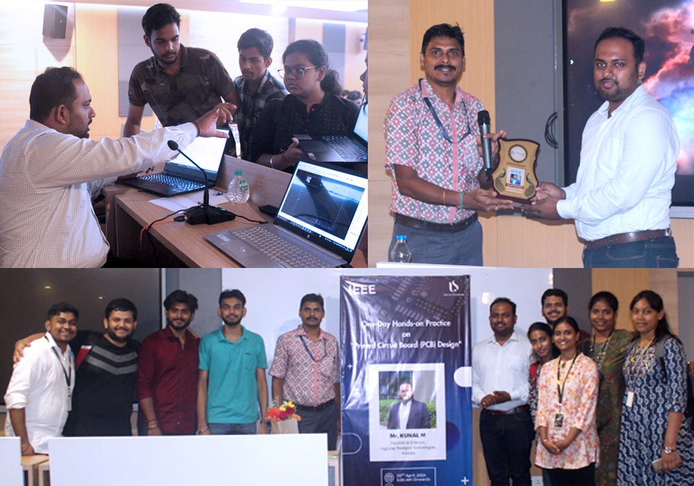
The Department of Electrical and Electronics Engineering (EEE) at SiliconTech, the engineering institute of Silicon University, collaborated with the Institute of Electrical and Electronics Engineers (IEEE) Students Chapter to organize a one-day hands-on session on ‘Printed Circuit Board (PCB) Design’ on 20 April 2024.
The objective of the session was to enable participants to grasp the best practices for designing a PCB layout, gain practical experience in designing single-sided and multilayer PCBs with Dual In-line Package (DIP) and Surface Mount Device (SMD) components, and comprehend the fundamental rules and files for PCB manufacturing.
The hands-on session was conducted by Mr. Kunal M, Founder & Director, Logiczap NextGen Technologies, Kolkata. He began the session with a brief introduction to software installation, component footprint, schematic diagram creation, basic software controls, and routing techniques. Participants acquired an understanding of both single-sided and multilayer PCB design processes. In the hands-on session, they successfully developed a multilayer PCB featuring DIP and SMD components for an adjustable voltage regulator, along with a single-sided PCB incorporating DIP and SMD components for an infrared sensor
A total of seventy three students participated in the session to acquire practical skills in designing both single-sided and multilayer printed circuit boards (PCBs). Additionally, they explored effective strategies for PCB layout design.